Hexawave continues to pursue innovation, empowering and inspiring the development of products. With a great deal of experience in the communication field, we pioneer the industry in undertaking strategic planning for emerging trends, technologies, and products.
5G Wireless Communication
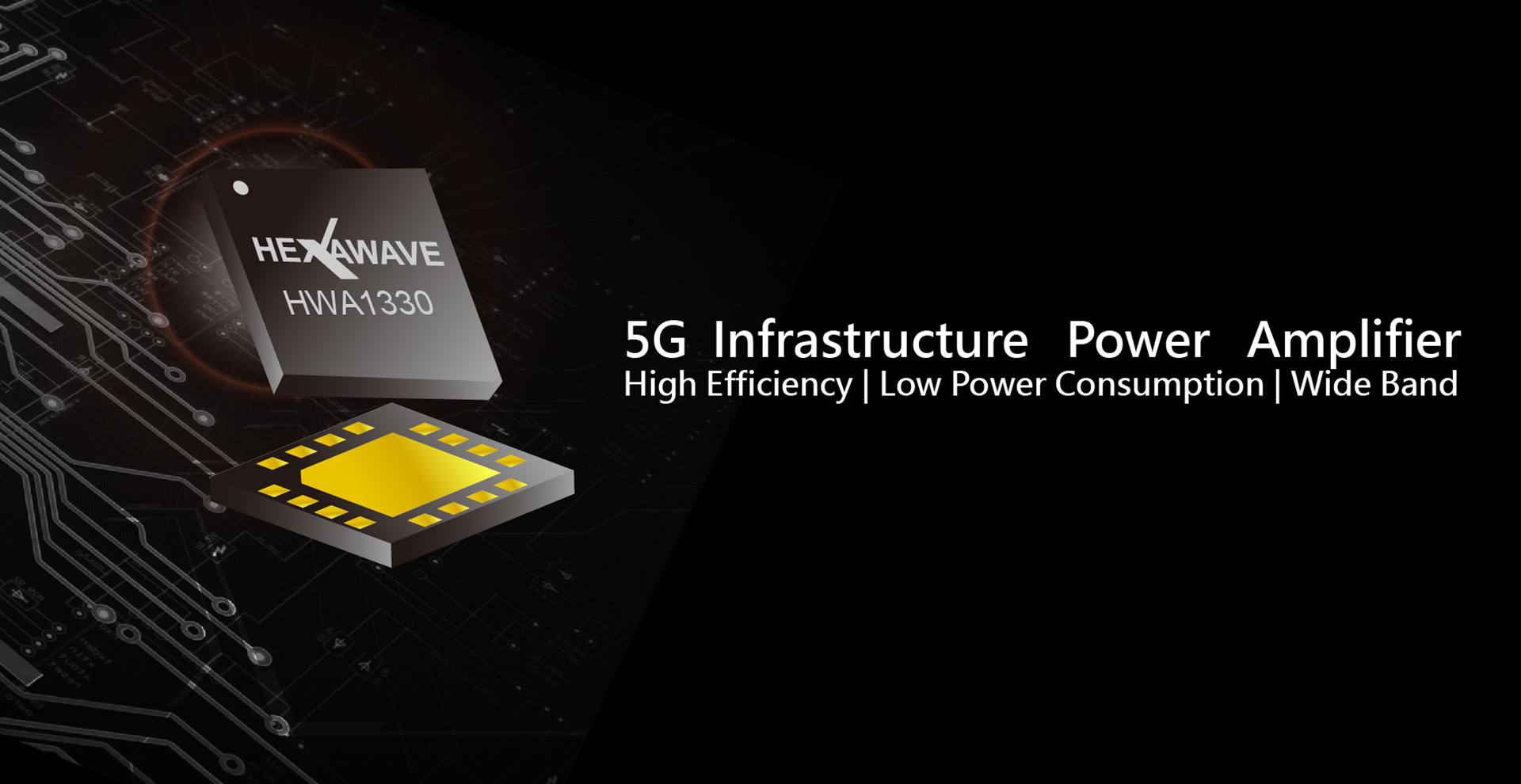
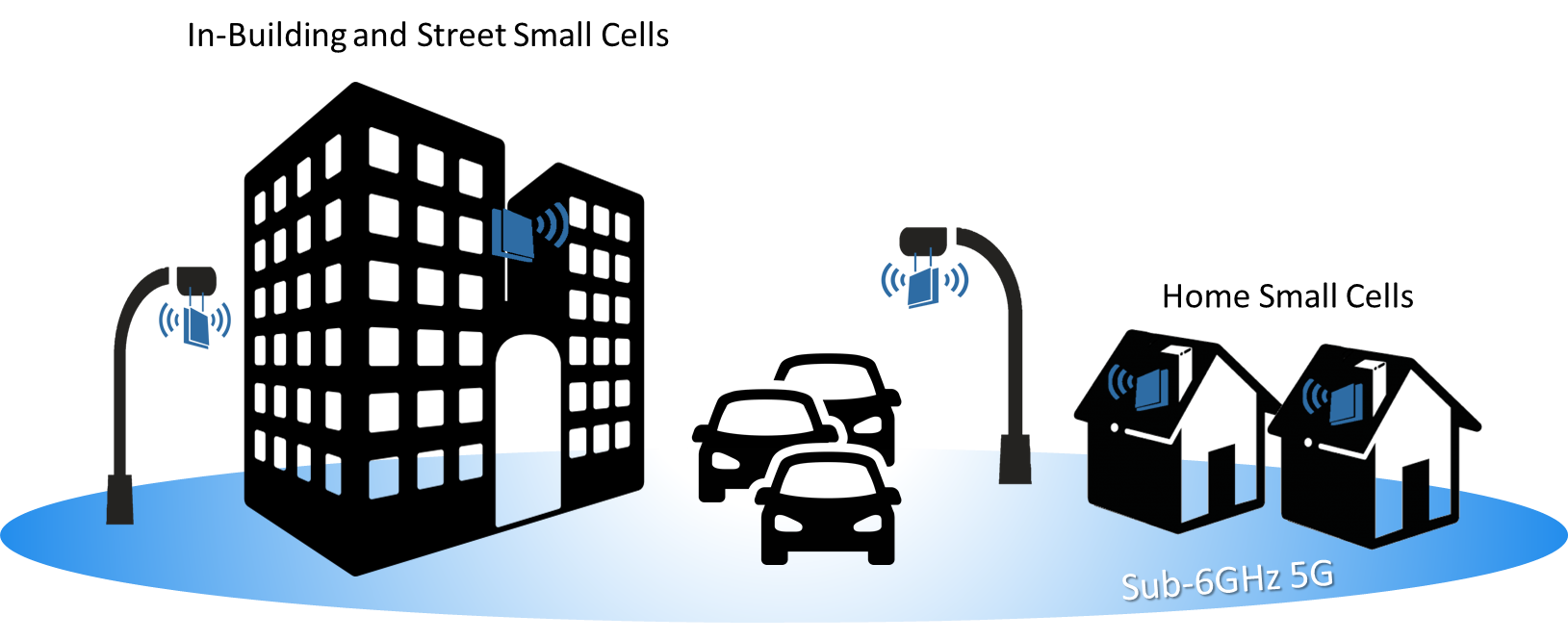
We strive to develop a series of high-gain and high-efficiency power amplifiers for 5G New Radio, which conform to the 5G New Radio FR1 frequency band formulated by 3GPP. Our product portfolio has diverse applications, including open wireless access network (O-RAN), Small Cell, repeater/DAS and general wireless applications, etc.
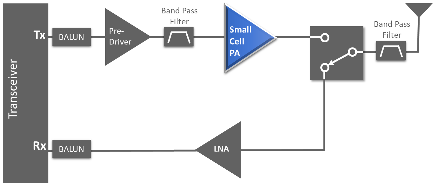
The power amplifiers (PA) are critical components in the wireless communication system. We have launched a series of high-gain and high-efficiency power amplifiers. The outstanding power-added efficiency (PAE) can greatly reduce the overall system power consumption as well as the cost of cooling devices. We can help customers effectively deploy dense 5G networks.
Featured Power Amplifier
Wide Band
High Power Added Efficiency
High Gain
High Linearity
Wireless Networking
Why Hexawave's RF Switch?
We provides a complete product line of RF Switches for wireless communications,microwave communications,and satellite communications. Hexawave uses proven GaAs pHEMT & IPD Technology to Serve the Market with High Frequency, High-Power, Low power consumption RF ICs.
High Frequency
Up to 8GHz
High Power
Up to 39dBm
Low Power Consumption
Less than 2uA
Variety of Package type
Meet Fluctuating demand
Featured RF Switch
IoT Sub-GHz Networking
Featured RF Switch for IoT
We provides a series of switches from SPDT to SP8T features Low Insertion Loss, High Isolation and High Gainfor Low Power Wide Area Networking applications.
| Part No. | Type | Frequency | Insertion Loss | Isolation | P1dB | Package |
| (GHz) | (dB) | (dB) | (dBm) | (mm) | ||
| HWS486 | SPDT Terminated Switch |
DC-6.0 | 0.5-0.6 | 22-29 | 36@+3V | USON6L (1.5x1.5x0.4) |
| HWS504 | SPDT | 0.5-6.0 | 0.4-0.5 | 20-23 | 32@+3V | USON6L (1.5x1.5x0.4 ) |
| HWS520 | SP3T | 0.5-6.0 | 0.5-0.9 | 25 | 30@+3V | USON8L (1.5x1.5x0.4) |
| HWS408 | SPDT | DC-3.0 | 0.4 | 25 | 30@+3V | SOT-363 (2.0x2.2x1.05) |
| HWS541 | SPDT | 2.0-6.0 | 0.35-0.55 | 25-27 | 31@+3V | LUSON6L (1x1x0.4) |
 256 bit SSL Encryption